References:
- PedalPCB Pauper build docs here: https://www.pedalpcb.com/product/pauper
- I get most of my parts from Small Bear:http://smallbear-electronics.mybigcommerce.com
- I don't need another overdrive. I already have a Strymon Sunset I'm pretty comfortable with, so I don't know why I'm doing this.
Perfboard Layout
I've already perfboarded a clone of the Colorsound one knob fuzz, so I felt ready. Was I wrong. The layout for this took me literally 20 hours, I’m not kidding. Drawing, erasing and redrawing to the point of nausea. Felt 10x harder than the little fuzz. It was a learning experience, and I will do better next time, but holy crap. The feedback loops around gain stage one were hard to map, and the output tone section was eye opening - look at those weird little loopy bits on the right side. This is a particular flavor of mental effort that I've never tried before - nothing in my life had prepared me for it.
Managing to put VREF (1/2 rail) in the places it was most needed was interesting. I couldn't get it from the pots to pin 5 of the op amp, so down below in the rear perfboard image you'll see little wires everywhere. In this layout, little wires are be required for:
- Tag A, going from stage one to stage 2
- Tag B, going from stage 2, to one side of the clipping section, and on to the tone section
- The VREF to the IC, as mentioned above
- Ground to the IC, and to the input common
Perfboard Solderjob (Front)
Note that my layout failed to account for the large size of the 100uf electrolytics, as well as the 1uf poly caps. The layout assumes that all resistors are loaded vertically and take just two adjacent holes, and that all caps take 3 adjacent holes - neither having much width. So you'll see my optimistic layout sprawls quite a bit when I got to the supply filtering (C10, C11).
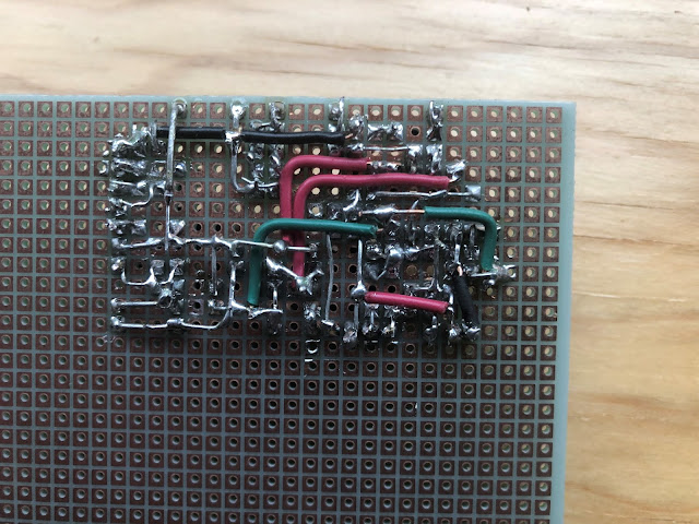
Perfboard Solderjob (Rear)
The solder side of the perfboard is a two layer wire superhell. I've seen other boards where people sort of draw traces on the pads, bridging them together in relatively neat lines. Haha lame! I solder the components in, then I bend all the wires over to touch each other. I used thicker leads from some weird old power resisters for the posts, and bridge the components to those. I'm not proud of it.
Control Layout (Front)
This is the what the front might look like. I'll do all the wiring on this jig so I don't have to work in a 125B enclosure. I'm bringing the dual gang DIP and internal treble trimmer out to the front, like a daft nutter. The only thing I'll have to solder when it goes into the real enclosure is the DC jack, which unfortunately has an internal nut.
Control Layout (Rear)
Here I've trimmed the board on a band saw with a metal cutting blade, so it fits easily in the 125B. All the jacks will go at the top (in/out/power). I've calculated that, in a perfect world, the plastic 1/4" box jacks will ride a couple of millimeters over the terminals of the left and right switches, while the 2-terminal power jack will clear the top of the center switch housing by a similar amount. My pedal calculations are often wrong. Yes, the left and right (canonically DIP) switches are SPDT here, which is an extra throw, but if this pedal doesn't work out, then...SPDTs are more versatile and cost very little more.
The plan is to wire up just the potentiometers and test. All of the switches have a default off position, so leaving them unconnected should put the Pauper/POT in "boost" mode for the first test.
I give this a 50% chance of being an undebuggable nightmare that I have to scrap in defeat. Witness me.


